74LVC1G08GW
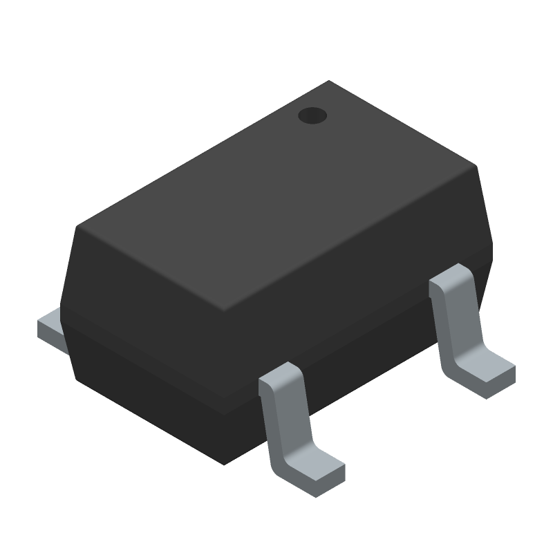
The 74LVC1G08GW is a 2-input AND gate from Nexperia, operating within a temperature range of -40°C to 125°C. It features a supply voltage of 1.65V to 5.5V, with a nominal voltage of 3.3V. The device is packaged in a TSSOP-5 package, measuring 1.25mm in width and 2.05mm in length. It is designed for automotive applications, meeting the requirements of the Temperature Grade: AUTOMOTIVE classification.
Similar Components
74HC165D,653
8-bit parallel-in, serial-out shift register with complementary outputs. Features positive edge triggering and rightward count direction. Operates within a supply voltage range of 2V to 6V, with a nominal 5V. Housed in a 16-pin SOIC package (R-PDSO-G16) measuring 3.9mm width and 9.9mm length. Supports a maximum operating temperature of 125°C and a minimum of -40°C, suitable for automotive applications. Propagation delay is 250ns with a load capacitance of 50pF.
74HC14D,653
CMOS Hex Schmitt Trigger Inverter IC featuring six independent inverter functions. Operating across a wide temperature range of -40°C to 125°C, this logic component supports supply voltages from 2V to 6V, with a nominal 5V. It offers a propagation delay of 190ns and is housed in a 14-pin SOIC package (JEDEC R-PDSO-G14) with dual terminal positions.
74HC595BQ-Q100,115
8-Bit Serial-In/Parallel-Out Shift Register, 16-Pin QFN, Automotive
74HC164
74HC164-Q100; 74HCT164-Q100 - 8-bit serial-in, parallel-out shift register TSSOP 14-Pin
PMV16XNR
PMV16XN - 20 V, N-channel Trench MOSFET TO-236 3-Pin
PESD5V0V1BL
The PESD5V0V1BL is a bi-directional transient voltage suppression (TVS) diode from Nexperia. It has a maximum working voltage of 5V and a maximum clamping voltage of 12.5V. The device features a low maximum leakage current of 0.01mA. It is available in a DFN package, suitable for surface mount applications. The PESD5V0V1BL operates over a temperature range of -55°C to 150°C.
About 74LVC1G08GW
The Nexperia 74LVC1G08GW Semiconductors datasheet provides detailed technical specifications, pinout information, and operating characteristics. This component: The 74LVC1G08GW is a 2-input AND gate from Nexperia, operating within a temperature range of -40°C to 125°C. It features a supply voltage of 1.65V to 5.5V, with a nominal voltage of 3.3V. The device is packaged in a TSSOP-5 package, measuring 1.25mm in width and 2.05mm in length. It is designed for automotive applications, meeting the requirements of the Temperature Grade: AUTOMOTIVE classification.. Key parameters include Eccn Code: EAR99, Family: LVC/LCX/Z, HTS Code: 8542.39.00.01, JEDEC Package Code: R-PDSO-G5, and Length: 2.05. 74LVC1G08GW is manufactured by Nexperia as part of their Semiconductors product line. On this page you can view and download the PDF datasheet, check specifications, and find similar components.
Specifications
- Manufacturer
- Nexperia
- Category
- Semiconductors
Ask AI Assistant
Ask questions about 74LVC1G08GW specifications
Click to ask a quick question:
Parameters
| Eccn Code | EAR99 |
| Family | LVC/LCX/Z |
| HTS Code | 8542.39.00.01 |
| JEDEC Package Code | R-PDSO-G5 |
| Length | 2.05 |
| Logic IC Type | AND GATE |
| Max Operating Temperature | 125 |
| Military Spec | False |
| Min Operating Temperature | -40 |
| Number of Functions | 1 |
| Number of Inputs | 2 |
| Number of Terminals | 5 |
| Propagation Delay (tpd) | 10.5 |
| REACH | Compliant |
| RoHS | Yes |
| Supply Voltage-Max (Vsup) | 5.5 |
| Supply Voltage-Min (Vsup) | 1.65 |
| Supply Voltage-Nom (Vsup) | 3.3 |
| Temperature Grade | AUTOMOTIVE |
| Terminal Position | DUAL |
| Width | 1.25 |